Tech
Intel’s Comeback Story Unfolds in Oregon Amid AI Chip Revolution
HILLSBORO, Oregon — Intel Corporation is reportedly on the cusp of a major comeback, driven by advancements in semiconductor technology at its Ronler Acres campus. This news comes as the chip industry adapts to the increasing demand for artificial intelligence applications.
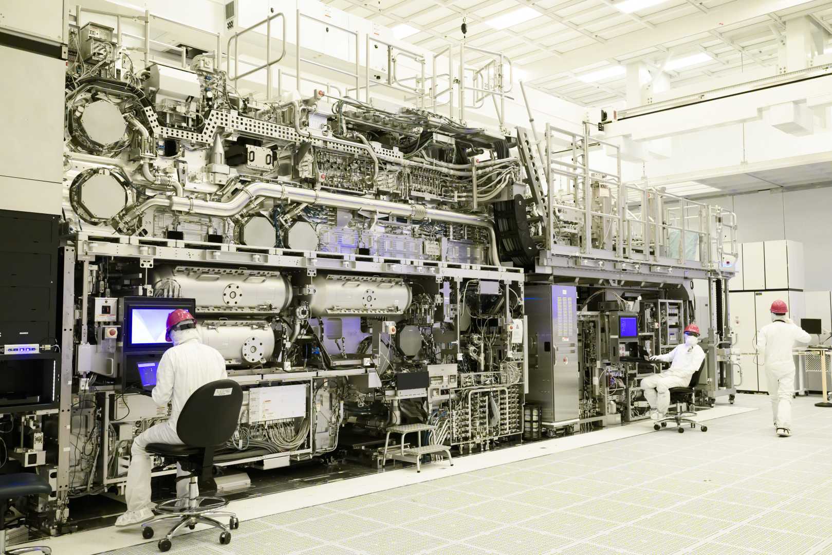
Despite facing skepticism just months ago regarding its production capabilities and technological roadmap, whispers from insiders suggest that Intel is significantly ahead of expectations. Key sources claim that Intel is leveraging High Numerical Aperture Extreme Ultraviolet (High NA EUV) lithography and Backside Power Delivery (BPD) technologies to enhance the production of its 18A chip processes.
Traditionally viewed as lagging behind industry leaders Nvidia and Taiwan Semiconductor Manufacturing Company (TSMC), Intel’s rumored advancements could reshape its competitive stance in the semiconductor landscape. The company hopes to deploy High NA EUV lithography for the 18A process, which could potentially give it a vital edge over competitors relying on established Low NA EUV technologies.
Intel CEO Pat Gelsinger has made aggressive moves, asserting the company’s commitment to reclaiming its status as a technology leader. “The second High NA tool is coming into our Oregon facility,” Gelsinger stated during a recent earnings call, indicating progress in the company’s timeline for advanced chip production.
These developments at Ronler Acres are being closely monitored, particularly as Intel may have secured a deal with Microsoft to produce AI chips. This partnership could be a significant validation of Intel’s overhaul efforts, providing them a vital customer and a path to increasing their production capabilities as demand rises for AI applications.
According to the cited insider, Intel’s integration of High NA EUV lithography not only streamlines chip manufacturing but could also substantially reduce costs. Intel managed to process more than 30,000 wafers in one quarter, showcasing dramatic improvements in manufacturing efficiency.
However, achieving such technological advancements involves navigating many challenges, including the complexities of integrating new machinery and materials. The expertise of Intel’s engineering teams will be crucial in ensuring that these new processes yield commercially viable products.
Intel’s Ronler Acres facility has been equipped with the latest EUV lithography machines, which are expected to facilitate the production of high-performance chips. If Intel’s progress aligns with current claims, it could potentially disrupt TSMC’s market dominance and enhance the semiconductor manufacturing presence on American soil.
As Intel aims to position itself as a credible competitor in the AI chip arena, industry watchers are keenly awaiting official confirmations regarding its strategic partnerships and production status. Any developments in the coming weeks will offer insights into the potential impacts on the broader technology market, particularly concerning AI capabilities shaped by changes in silicon technology.


